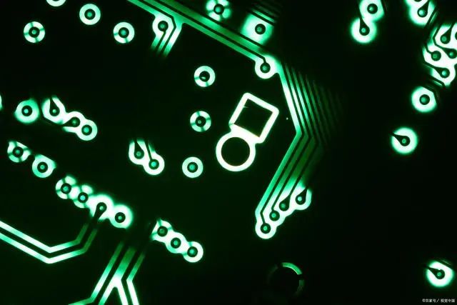
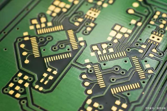
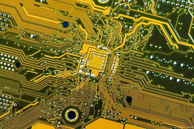
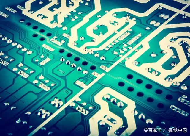
PCB (Printed Circuit Board) is no longer unfamiliar to us. It is the core component of electronic devices such as mobile phones, computers, radios, and lights. Without the development of circuit boards, we cannot enjoy the convenience brought by these electronic devices. Various types of printed circuit boards, such as rigid circuit boards, rigid flexible composite boards, multi-layer circuit boards, and high-density circuit boards, have been widely used in the market and have undergone multiple evolutions.
 In the embryonic stage (1900s 1920s):
In 1903, the famous German inventor Albert Hanson applied for a British patent. He pioneered the concept of using "wires" in telephone switching systems, using metal foil to cut line conductors. The top and bottom of the line conductors were coated with paraffin paper, and through holes were set at the intersections of the lines to achieve electrical interconnection between different layers. This is different from our modern circuit board manufacturing methods, when phenolic resin was not yet invented and chemical etching technology was not yet mature. The method invented by Albert Hansen can be said to be the embryonic form of modern circuit board manufacturing, laying the foundation for future development.
 Development stage (1920s 1940s):
In 1925, Charles Ducas from the United States came up with an innovative idea, which was to print circuit patterns on insulating substrates and then electroplate them to make conductors for wiring. The term "PCB" came into use at this time, making it easier to manufacture electrical appliances.
In 1936, Dr. Paul Aisler, an Austrian known as the "father of printed circuits," published foil technology in the UK and developed the first printed circuit board for use in radios. The method used by Dr. Paul Eisler is very similar to the method we use today for printed circuit boards. This method is called the material reduction process, which can remove unnecessary metal parts. Around 1943, Paul Eisler's technological invention was widely used by the United States to manufacture proximity fuze for World War II. At the same time, the technology was widely used in military radio.
 Turning Point (1948):
1948 was a turning point in the historical development of circuit boards, and the United States officially recognized that the invention of printed circuit boards could be used for commercial purposes. At that time, there was little history of electronic devices using circuit boards, but this decision greatly promoted the development and application of circuit boards.
Prosperity stage (1950s-1990s):From the 1950s to the 1990s, the PCB industry formed and grew rapidly, which was the early stage of PCB industrialization. At this time, PCB had become an industry. In the 1950s, the electronic market began to use transistors, effectively reducing the size of electronic products and making it easier to integrate circuit boards. In addition, the reliability of electronic products was significantly improved.
In 1953, Motorola developed a double-sided board with electroplated through holes. Around 1955, Toshiba Corporation of Japan introduced a technology to generate copper oxide on the surface of copper foil, and copper clad plates emerged. It was precisely because of these two technologies that multi-layer printed circuit boards were successfully invented and widely applied.
In the 1960s, printed circuit boards were widely used and circuit board technology became increasingly advanced. Thanks to the widespread use of multi-layer printed circuit boards, the ratio of wiring to substrate area was effectively increased.
In the 1970s, multi-layer circuit boards developed rapidly, pursuing higher precision and density, small holes, exquisite lines, high reliability, low cost, and automated production. At that time, circuit board design work was still done manually. Circuit board design engineers use colored pencils and rulers to draw circuits on transparent polyester film. In order to improve drawing efficiency, they have made several packaging and circuit templates for some commonly used devices. In the 1980s, surface mount technology gradually replaced through hole mount technology as the mainstream, and circuit board technology also entered the digital era.
Maturity stage (1990s to present):With the development of electronic devices such as personal computers, CDs, cameras, and game consoles, significant changes have occurred, and it is necessary to reduce the size of circuit boards to adapt to these small electronic devices. The digital design of circuit boards has achieved automation in many steps, making the design of small and lightweight components easier. As for component suppliers, they also need to improve their designs by reducing electricity consumption, and they also need to consider reducing costs.
In the 2000s, circuit boards became increasingly complex, with more and more functions and smaller sizes. Especially the design of multi-layer and flexible circuit boards makes these electronic devices more practical and practical, with smaller circuit board sizes and lower costs.
In the early 21st century, the emergence of smartphones led to the development of high-density circuit board technology. While retaining laser punched micro vias, stacked vias began to replace staggered vias, and combined with "arbitrary layer" construction technology, the final high-density circuit board line width/line spacing reached 40 μ m。 This arbitrary layer method is still based on the subtraction process, and it can be confirmed that for mobile electronic products, most high-end high-density circuit boards still use this technology. However, in 2017, high-density circuit boards began to enter a new stage of development, shifting from a reduction process to a process dominated by graphic electroplating.
Looking back at the development process, with the continuous progress of science and technology, the circuit board industry is constantly updating and evolving, and circuit boards play an important role in today's era. With the continuous emergence of electronic product applications in the consumer market, such as wearable electronic devices, electronic hearing aids, blood glucose meters, electric vehicle intelligent devices, aerospace and other fields, people have put forward higher requirements for the design, materials, and manufacturing of circuit boards.
Source: Lao Zhao said manufacturing
Statement: We respect originality and also value sharing; The copyright of the text and images belongs to the original author. The purpose of reprinting is to share more information and does not represent the position of our account. If there is any infringement of your rights, please contact us promptly and we will delete it as soon as possible. Thank you